
The Concept
Integrated electronic systems are becoming increasingly important and complex in today's world. In this process, engineers work together in a division of labor, creating IP blocks according to well-defined specifications. By assembling many individual blocks, the ASIC is created.
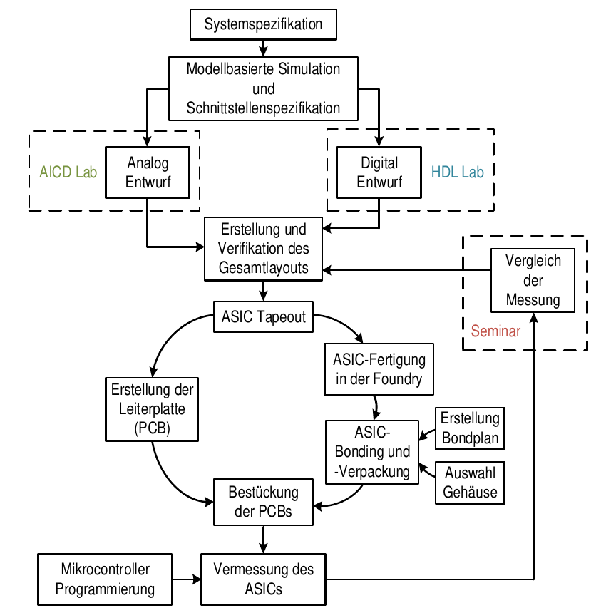
We at the department want to illustrate the chip design as practically as possible in order to prepare the student in the best possible way for later activities in the field of semiconductor development. The stages of the development process from initial specifications to a manufactured functional chip are represented by our diverse courses.
Design, simulation and verification of analog and digital circuits are performed in the AICD Lab and HDL Lab. Designs are matured to the point where they meet all requirements for fabrication. The students can then test the externally manufactured chips in seminars. For this purpose, special test boards are manufactured and the chips are measured in the lab.
The Chip
The enormous complexity of today's state-of-the-art integrated circuits, based on decades of experience of numerous engineering teams, is not difficult to achieve. Nevertheless, we want to offer more than a purely academic exercise. We enable the interaction of analog and digital circuitry with software for a realistic design task.
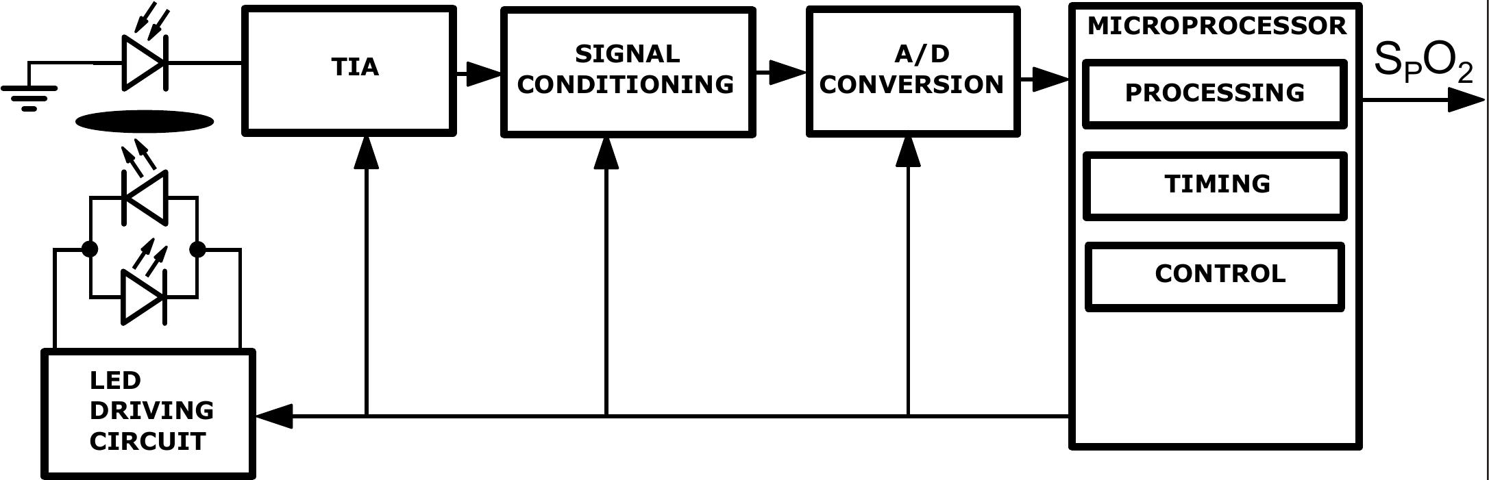
The pulse oximetry method already used in the medical technology practical course serves as motivation. In this process, students can use LEDs to measure their pulse in a non-hazardous way. Instead of a discrete design as used in the medical technology practical course, we aim for an integrated design that combines all relevant functions on less than 1 mm2 chip area. However, the hardware can generally be used for a wide variety of sensor signals.
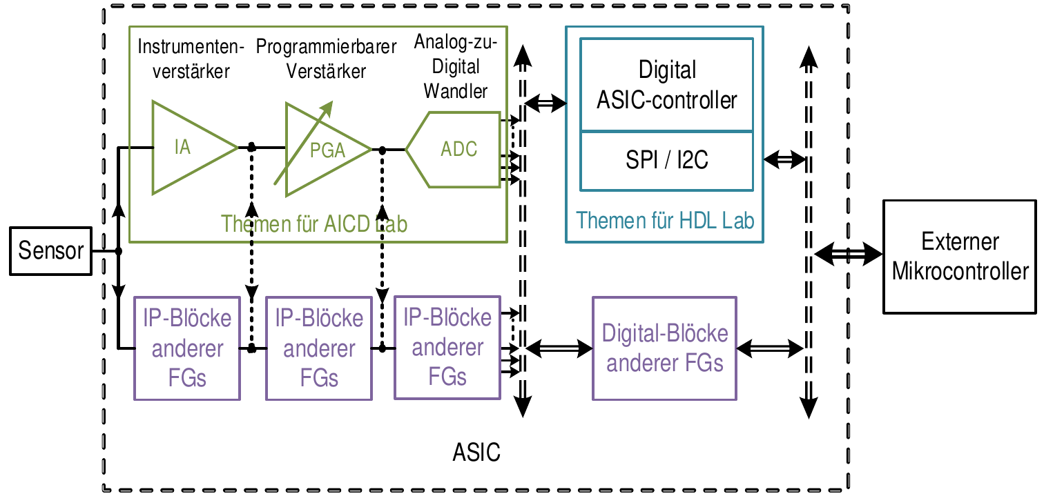
On the chip we combine the works of students from different courses to the complete system. The analog IP blocks are developed within the AICD Lab. These process an analog sensor signal and convert it to a digital representation. The digital IP blocks are developed within the HDL Lab. These evaluate the digitized input signal to extract information such as pulse and oxygen saturation.
AICD Lab
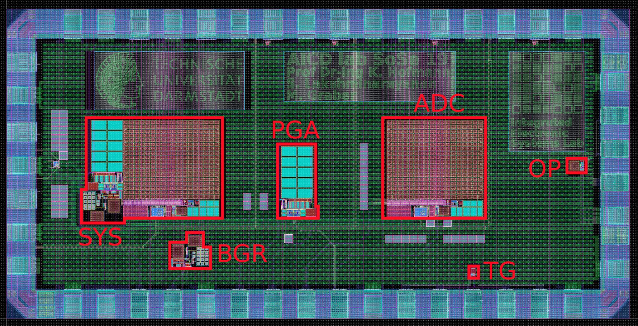
Three IP blocks are defined for the analog signal chain. As part of the AICD Lab, students develop one of these IP_blocks of their choice in groups of two.
The input signal is first amplified by a programmable gain amplifier (PGA). The gain can be adjusted in 3dB steps by the digital part and an active anti-aliasing filter can be switched on. A bandgap reference provides a stable and accurate reference voltage to enable analog to digital conversion. Using this reference voltage, an 8-bit SAR-ADC digitizes the analog sensor signal amplified by the programmable gain amplifier. The resulting digital representation of the input signal is made available for further digital circuits. At the same time, the analog signal chain can be adjusted by setting the gain.
The input signal is first amplified by a Programmable Gain Amplifier (PGA). The gain can be adjusted in 3dB steps by the digital part and an active anti-aliasing filter can be switched on. A bandgap reference provides a stable and accurate reference voltage to enable analog to digital conversion. Using this reference voltage, an 8-bit SAR-ADC digitizes the analog sensor signal amplified by the programmable gain amplifier. The resulting digital representation of the input signal is made available for further digital circuits. At the same time, the analog signal chain can be adjusted by setting the gain.
HDL Lab
In the HDL Lab, the digital design flow for the pulse oximeter is performed.
For this purpose, various circuit blocks such as an FIR filter or the digital control unit are developed in Verilog (Hardware Description Language-Lab). The FIR filter removes the high frequency components of the input signal. The digital control unit takes over the control of various circuit blocks developed in the AICD Lab, such as the programmable gain amplifier (PGA) and SAR-ADC.
During development, the written code must be verified by the students in various testbenches. Mixed signal simulations (AMS) are also performed to ensure that the analog part designed in the AICD Lab works properly with the Verilog code written in the HDL Lab. If verification is successful, the Verilog code is synthesized using Synopsys Design Vision. In this process, the written Verilog code is translated into a schematic with logic gates. After successful synthesis, place and route is performed using Cadence Encounter. In this step, the previously generated schematic with logic gates is converted into a physical layout.
Tapeout
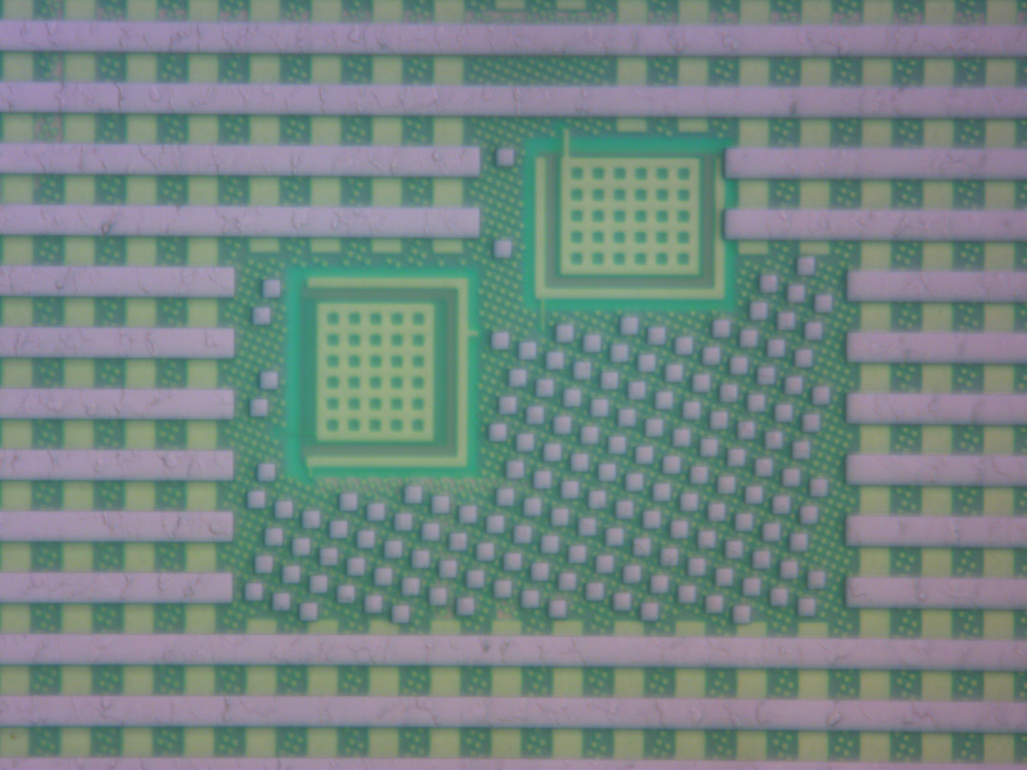
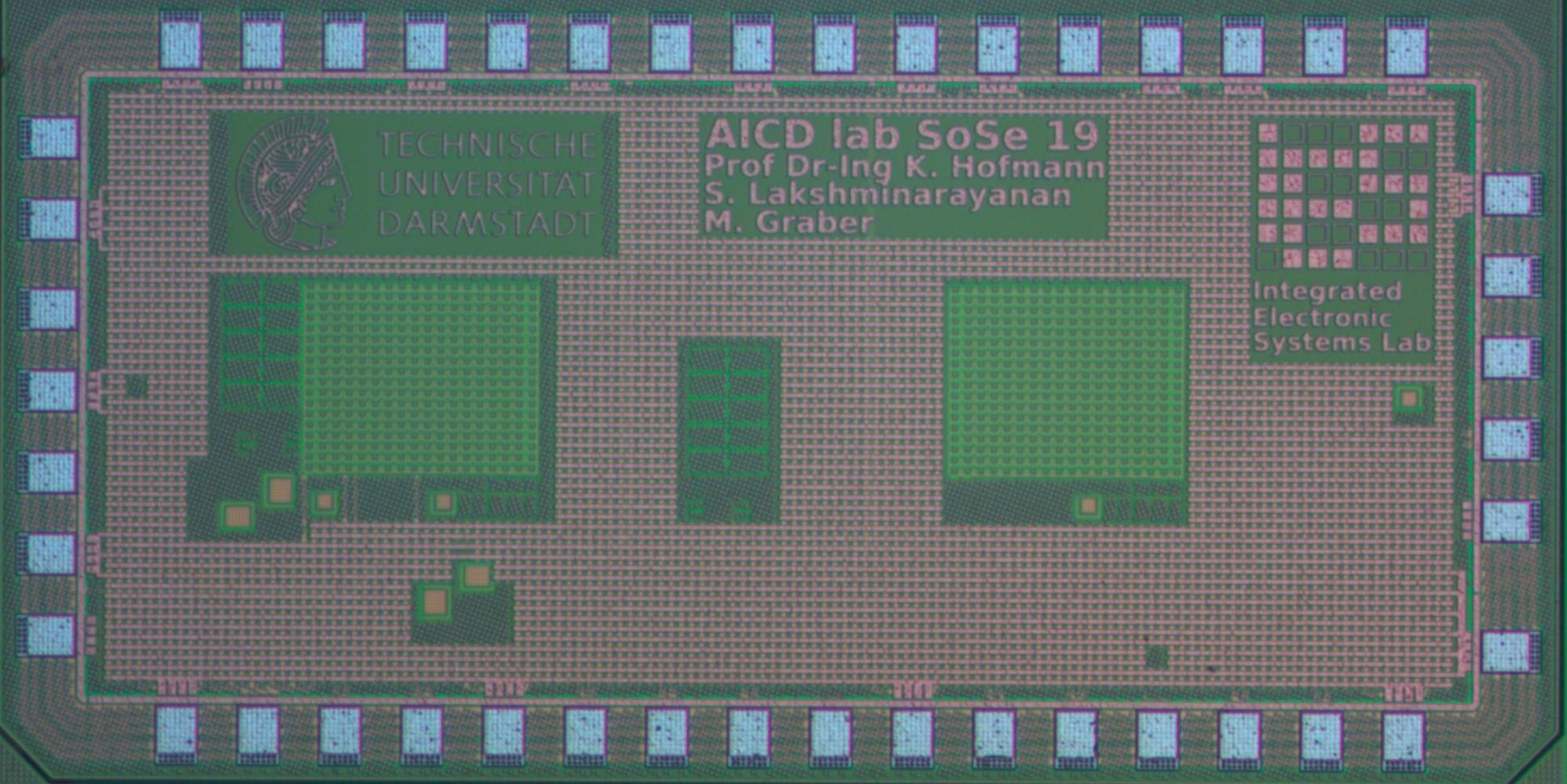
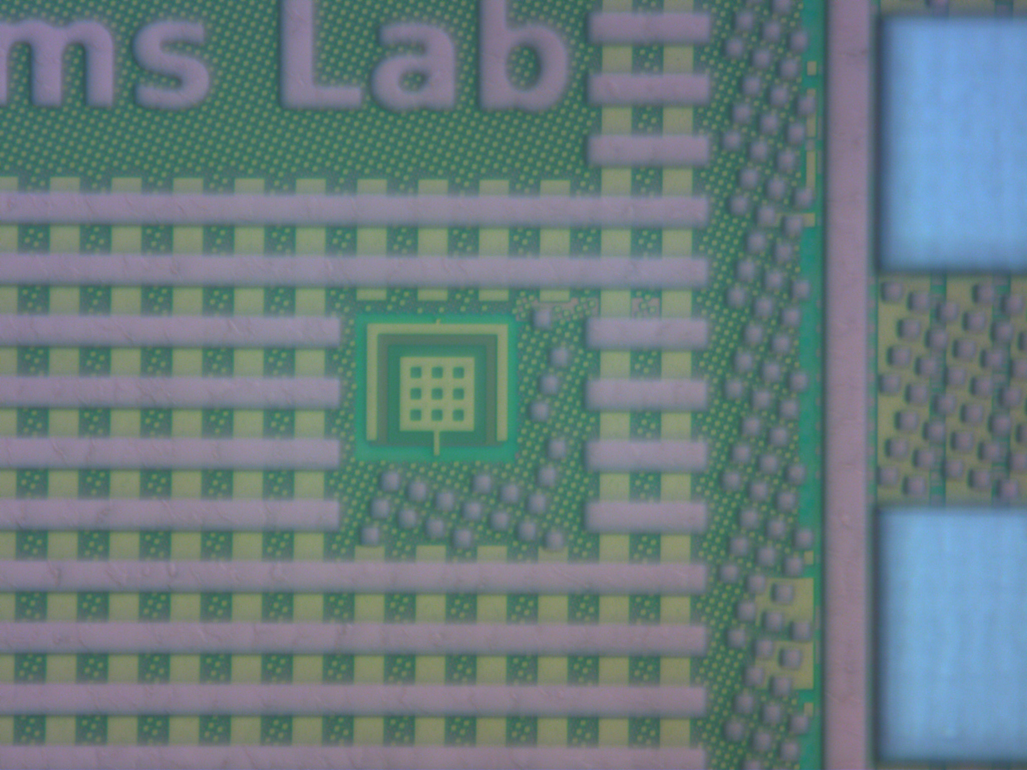
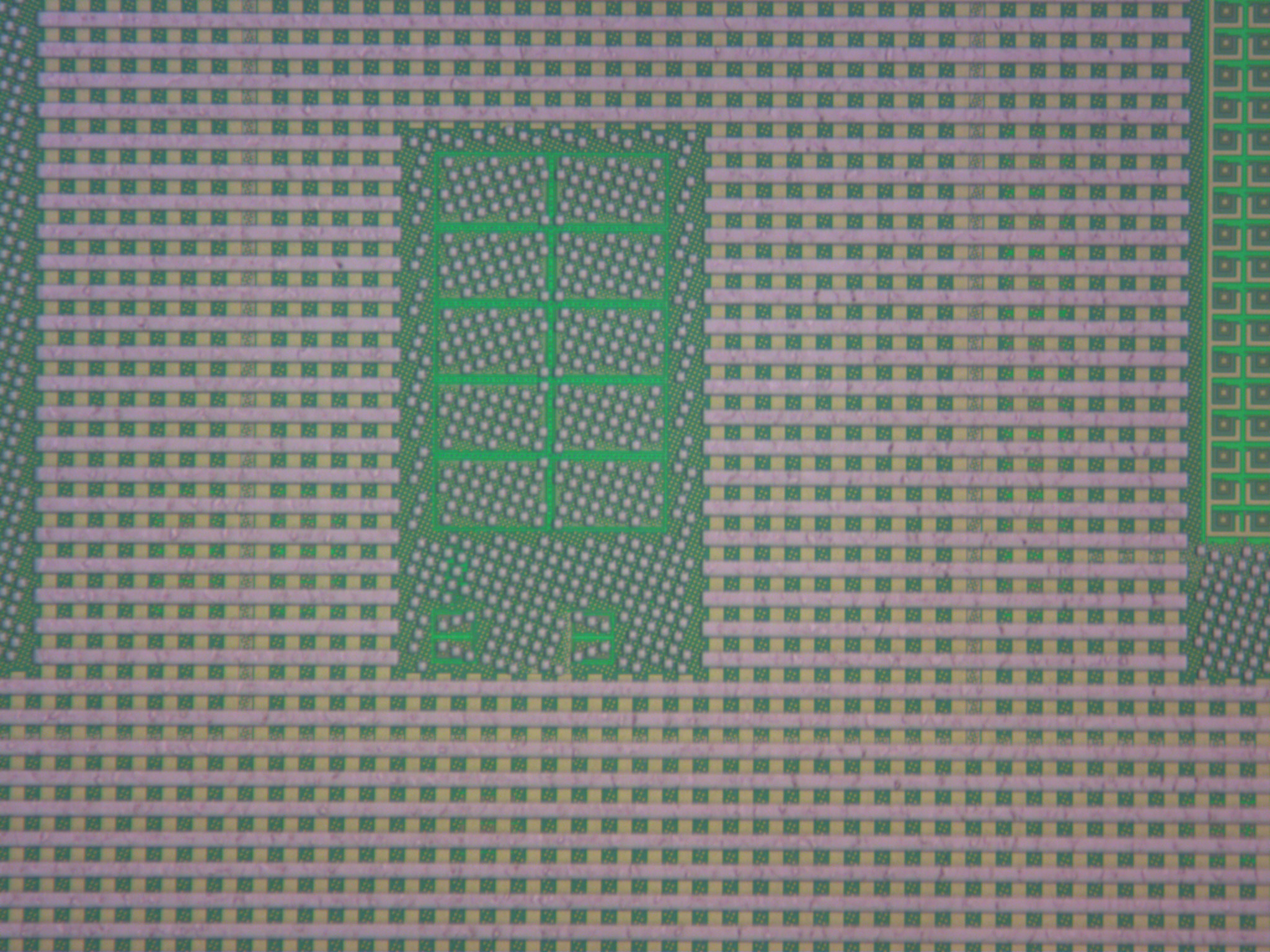
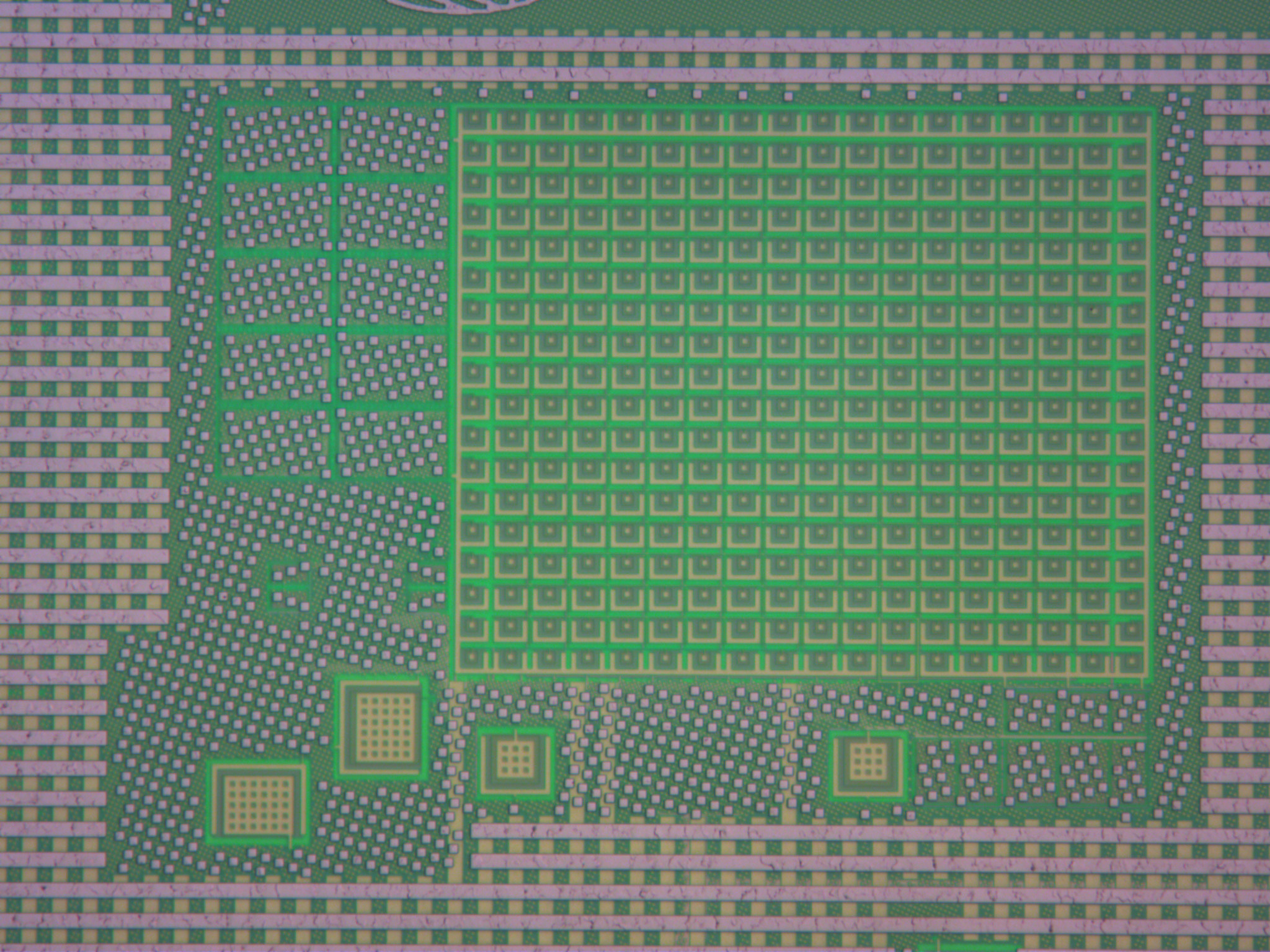
Following the lecture period, the chips are manufactured. The designs are simulated in detail post-layout to test them for robustness in case of manufacturing inaccuracies. The chip shown here occupies less than 1 mm2 of area, while the size of the actual circuit is much smaller. Additional structures such as IO cells with ESD protection and pads for electrical contacting are added. Under the microscope, the chip compares nicely with the layout data.
Measurements
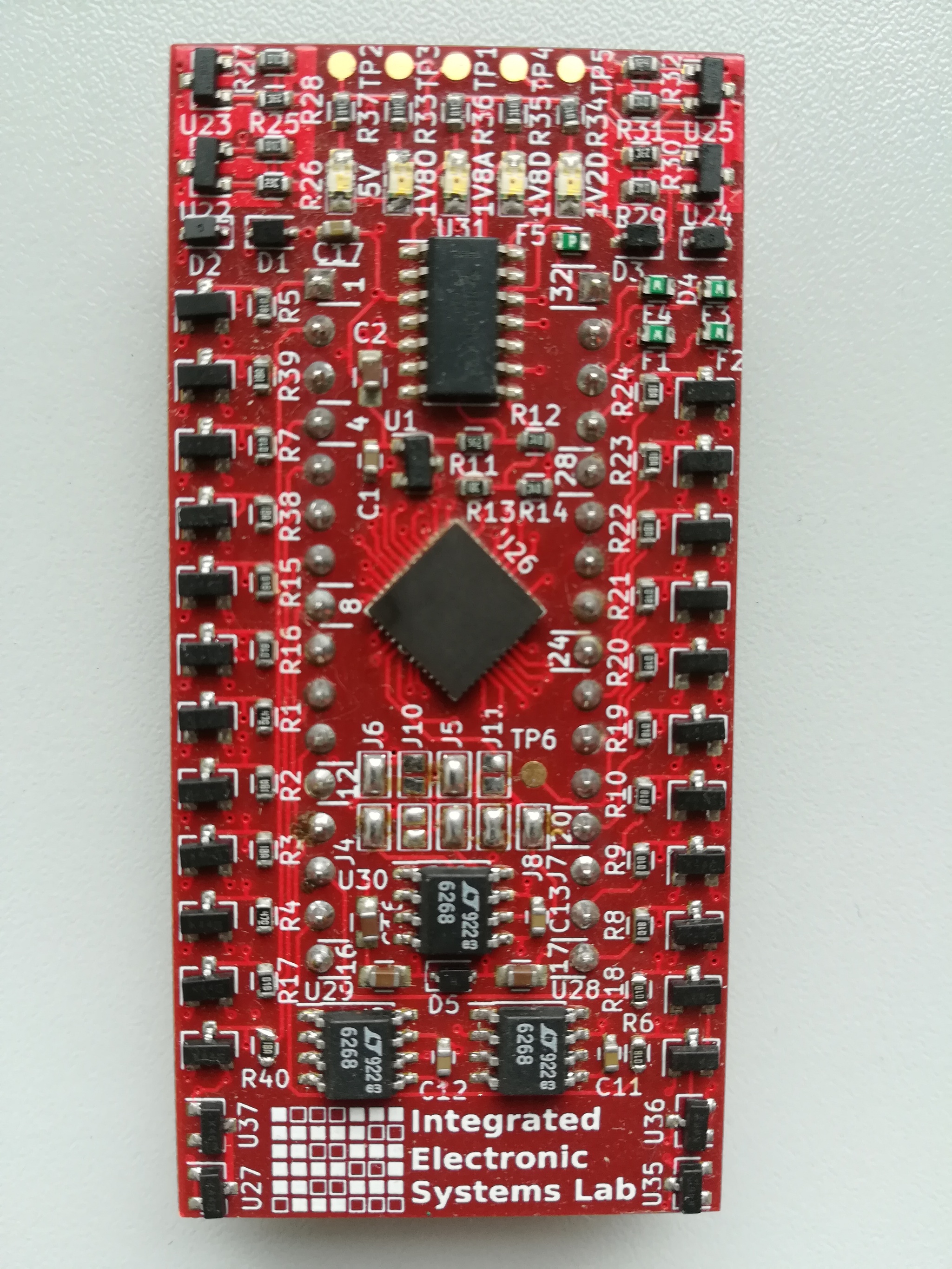
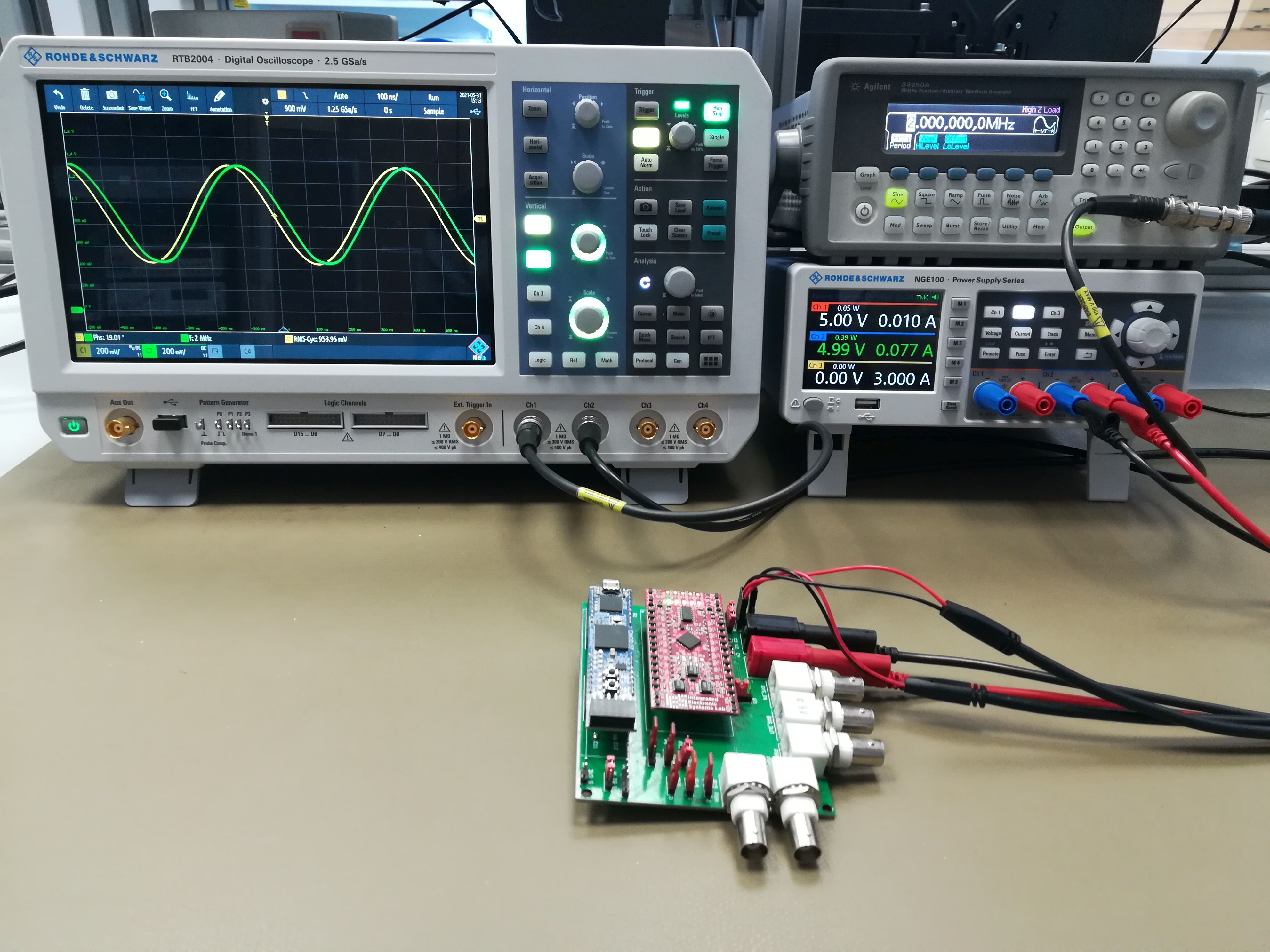
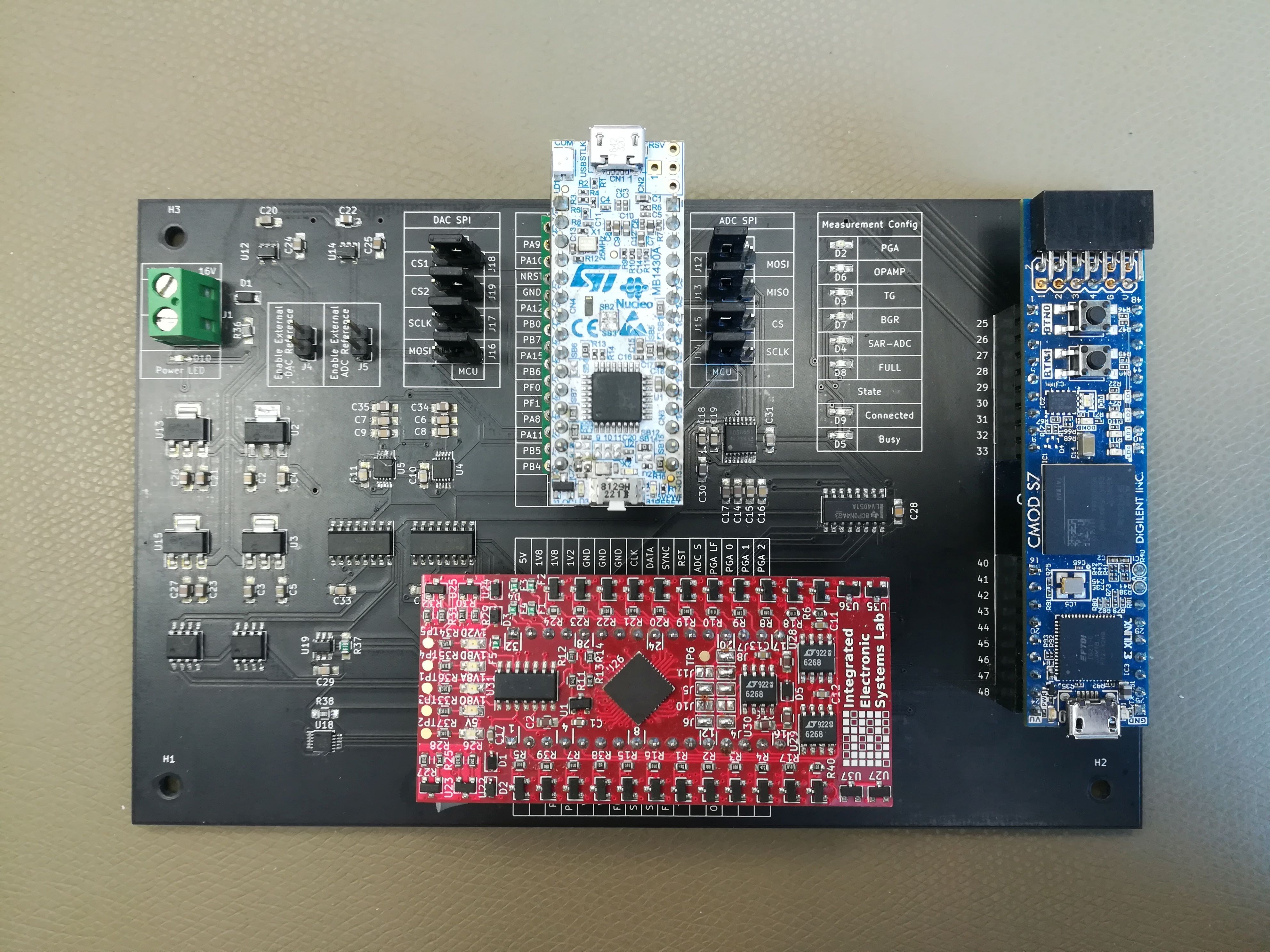
The manufactured chips can then be measured in our laboratory. The first step is to manufacture a circuit board that supplies the chip with voltage and connectors for connection. For measurements, the handling of laboratory measuring instruments such as oscilloscope, function generator and laboratory power supply is necessary. In addition, post-processing and evaluation are an integral part. The measured values obtained can be compared with the simulated values and causes for deviations can be identified.
Platform for further designs
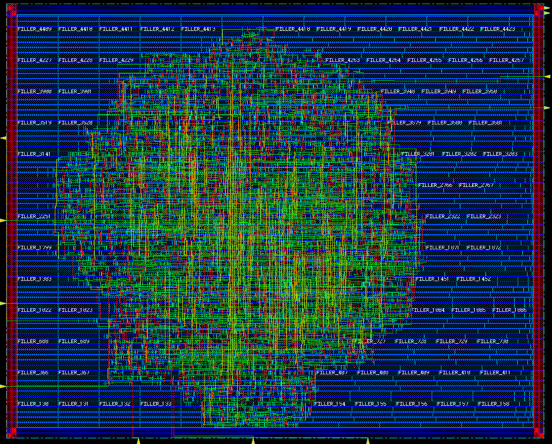
The circuits developed at IES occupy only a small part of the available chip area in the UMC 65nm low leakage technology used. A large part of the area is only provided with a power grid and fillers to get the manufacturing compliant solution.
Therefore, there is a possibility for other colleges/universities from the state of Hesse to add their own circuit parts. These can share our existing circuits or work independently using their own IO pads. For inquiries in this regard please contact Prof. Dr.-Ing. Klaus Hofmann.