High Speed Measurements on Memristors
So far, memory manufacturers can only dream of memory devices that are non-volatile, fast and durable. And so do we: Doesn’t it happen way too often that the coffee machine wastes valuable seconds in the morning, just for booting? Wouldn’t it be nice if all our appliances would begin their work without taking their own time to wake up?
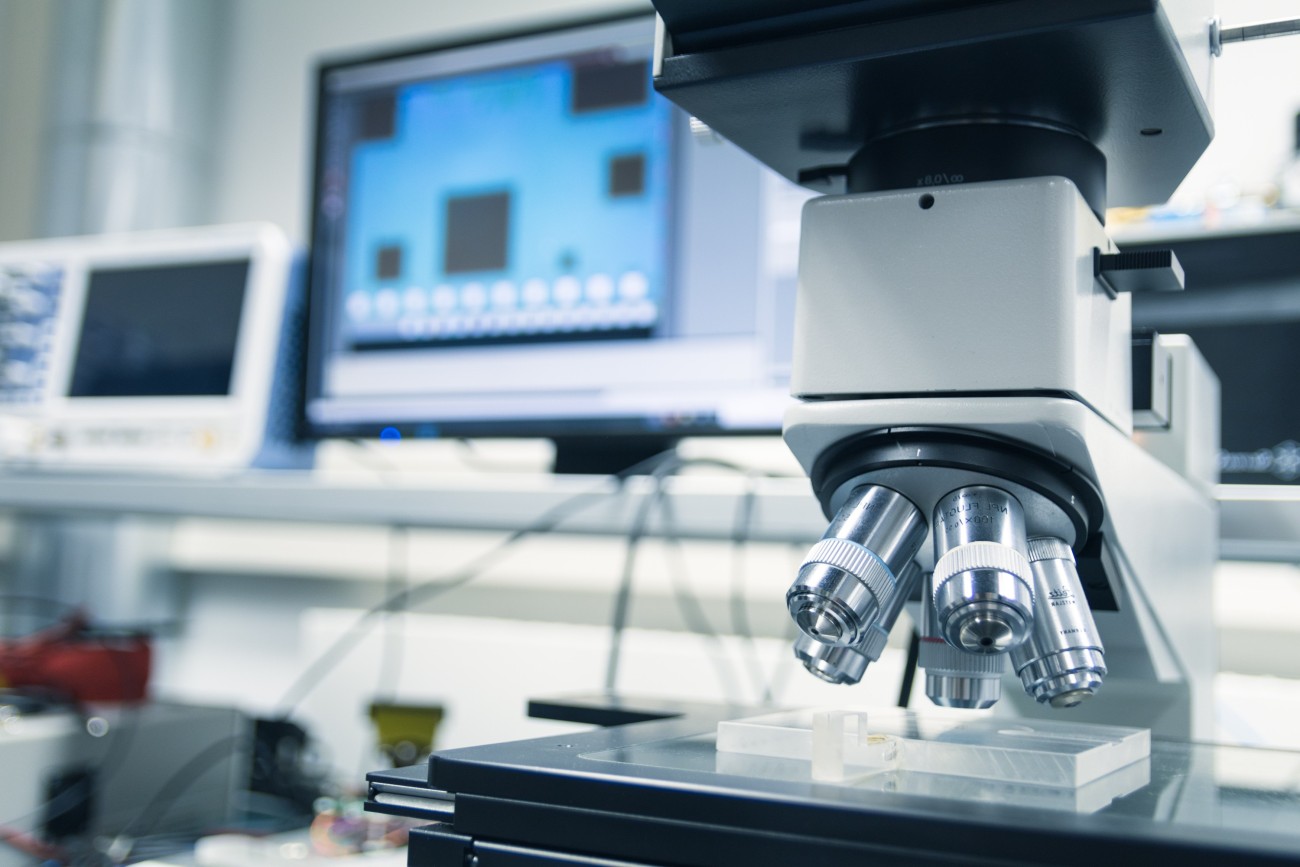
For this, new memory components are needed, and memristors can fulfill these requirements. Applying voltage pulses changes their resistance value, which can then be used for storing information. In our lab, we use Y2O3 -memristors; and since their internal processes happen very quickly, we are conducting measurements with high bandwidths. We use a self-developed measurement system that permits the simultaneous acquisition of current- and voltage waveforms – with a time resolution of only one nanosecond. Accurate models of our test setup play a crucial role for reaching the required precision.
The knowledge that we gain about these new devices helps understanding how new memory technologies can be improved – and in the end, they might just find their way into our everyday life.
Oscillator-based Ising Machines
A lot of applications in industry, economy, and science need to solve optimization problems. Examples are the flight schedule of airlines, production planning in factories, or research on new molecules. Unfortunately, the runtime for solving such problems grows exponentially with size. In practice, this means, that the time needed for obtaining a solution explodes. Therefore, much faster and efficient approaches are needed, than classical processors can provide.
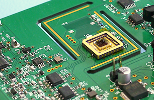
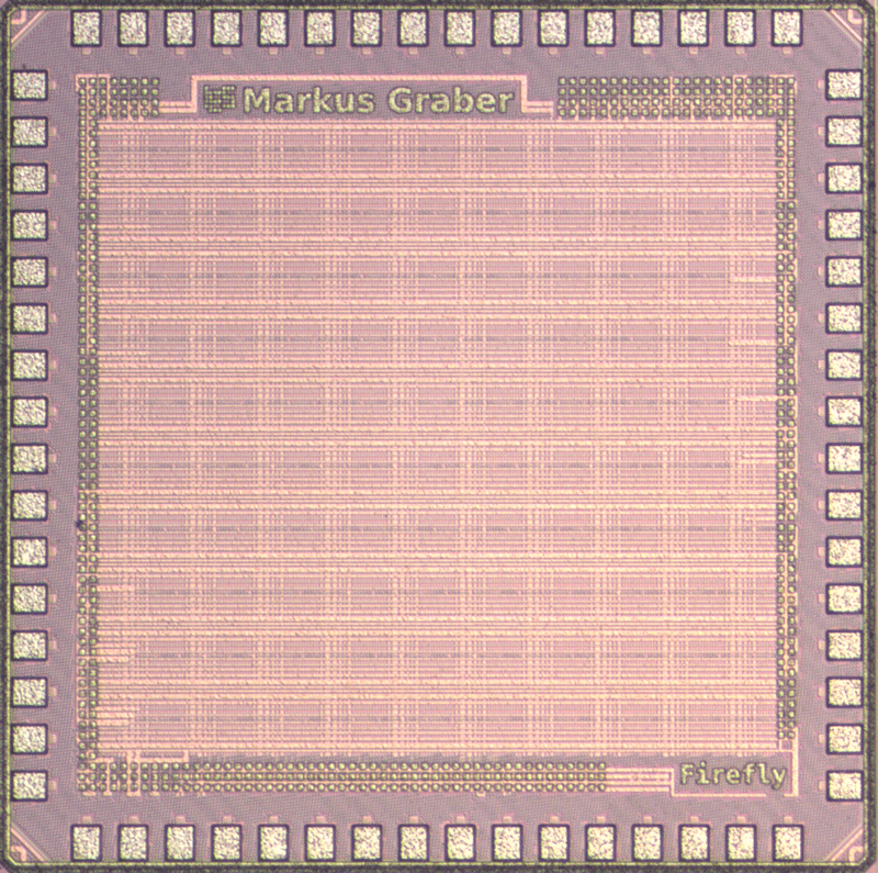
Our research focuses on so-called oscillator-based Ising machines, which specialize in solving optimization problems in an Ising Form. Instead of using resource-costly algorithms, which are executed using trillions of transistors, we want to leverage the physical nature of the devices directly for the computation. We are researching special, configurable systems of coupled oscillators, which have a natural tendency based on their synchronization to seek a ground state. As part of our research activity, we successfully developed and lab-tested two generations of ASICs, which contain more than a thousand oscillators on just a few square millimeters.
Sensor-integrating Machine Elements
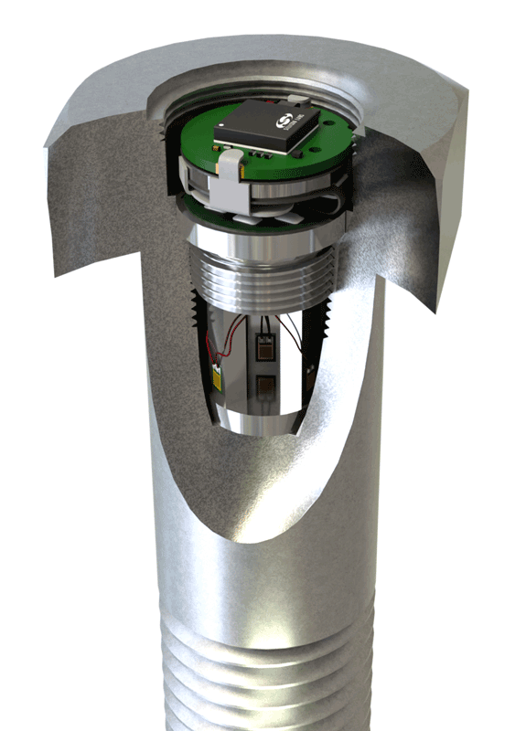
In the DFG project SiSmaK as part of the priority program 2305, we are working in cooperation with IPEK (KIT) and MUST (TUDa) on the integration of electronics and sensor technology in machine elements.
Using the example of an M20 screw, we are developing an energy-autonomous and room-neutral sensor platform for measuring multi-axial loads. Various communication and energy transmission concepts are being evaluated and a new ultrasound-based method based on an ASIC is being developed.
The Future of Integration
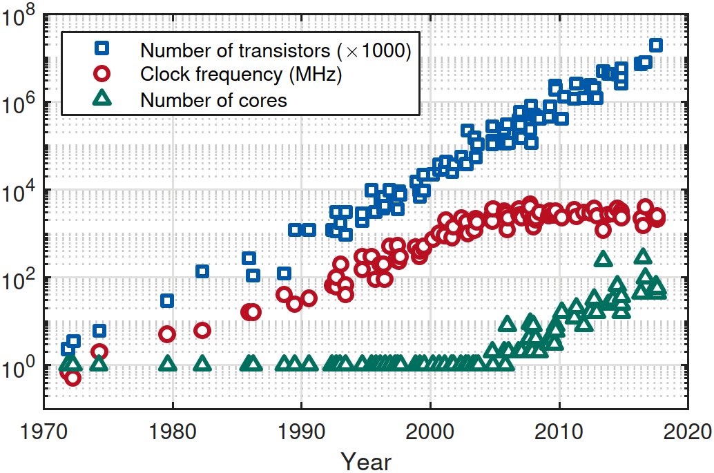
The developments of the last decades have shown that not all integrated circuit (IC) performance metrics maintained an upward trend. The exponential increase of transistor density in ICs has often been denounced with a pessimistic outlook for the future, and even today we assume a finite integration density in view of the physical limits. Similar to the plateau in clock frequency reached around 2005, we can expect to reach a maximum transistor density in the future.
Abstracted from transistor density, functionality per area is a fundamental criterion for performance, not only in the semiconductor domain. Miniaturization also plays an important role at system level and in mechanical processes. The department Integrated Electronic Systems is working on the future of various types of electronic systems and is researching sustainable concepts for the integration of electronics, which are outlined below.
Databelt
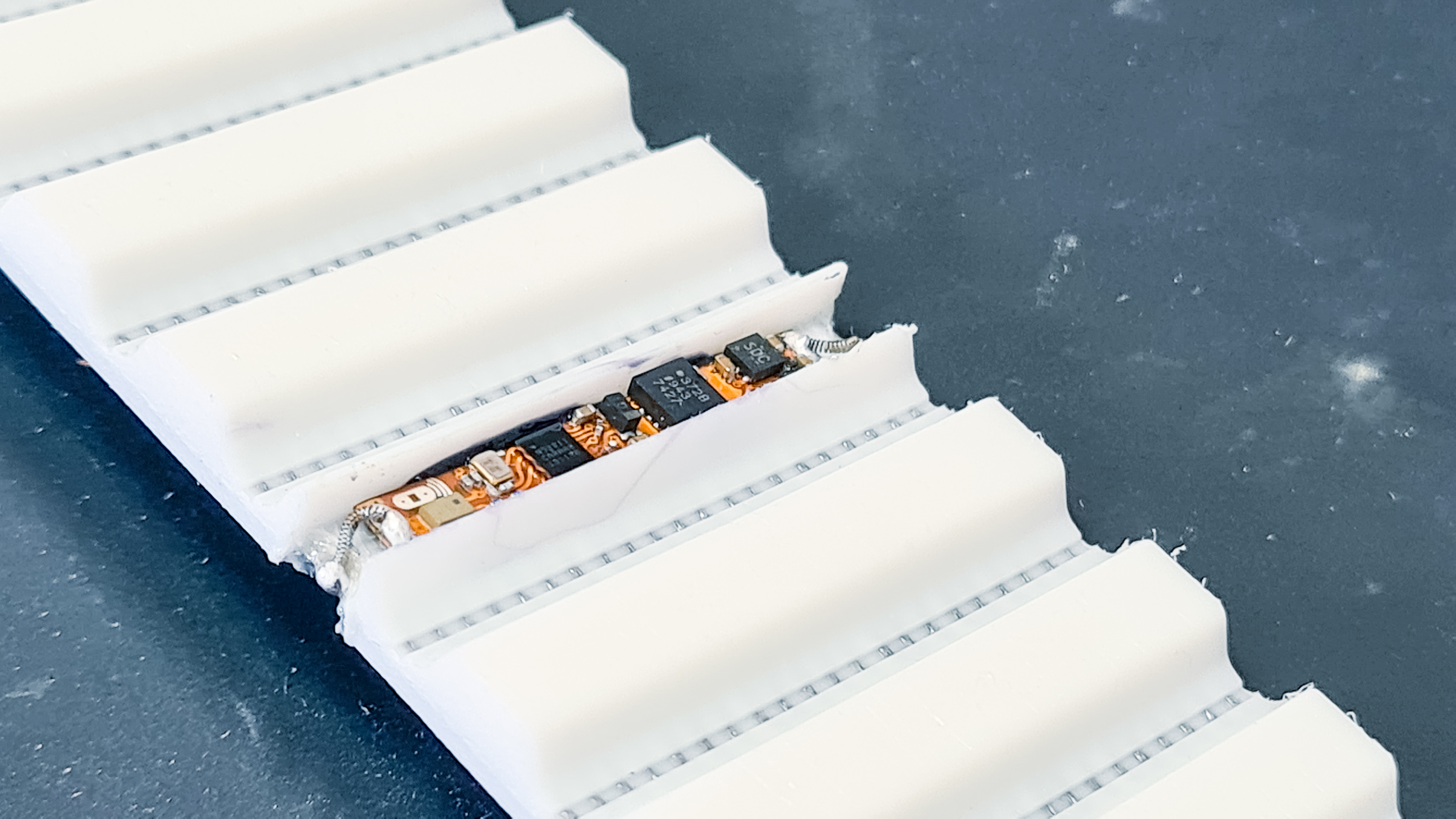
In the “Databelt” project, a measuring system is being developed that allows to collect measured values within a toothed belt and to send them to an external location during operation.
Such a measuring system enables the condition of the timing belt to be monitored during operation and is therefore a further step towards fully networked production. The main focus is on the wear of the timing belt, since this can currently only be determined with great difficulty by personnel on site. The tension force of the toothed belt, which is determined indirectly from its natural frequency, and the temperature inside the belt serve as indicators.
To record these two measured variables, a sensor node was developed which is small enough to be inserted into a tooth of the toothed belt.
Combined Fiberoptics Transmission Line
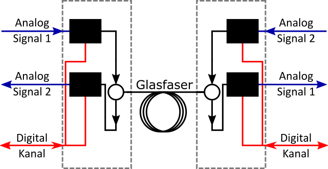
Despite the ever-increasing digitalization, broadband analog signals are still very common and irreplaceable in some applications. To transmit these signals over longer distances, there are solutions based on fiber optics.
A disadvantage of these solutions is the lack of data channels for system diagnosis and control tasks, which so far require additional fiber or other optical bands. For reasons of system efficiency, research is being conducted on a combination of analog and digital data channels over a single optical signal path.
This combination will enable more cost-effective and at the same time more flexible data transmission paths.
Ultrasonic Experimental Platform
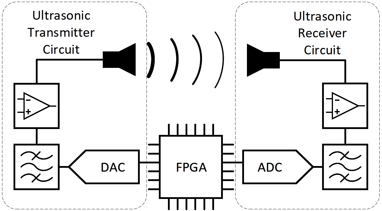
In times of Industry 4.0 and Predictive Maintenance, precise, robust ultrasonic sensors and their control gain importance. The circuit board developed at IES serves as experimental platform for 300kHz ultrasonic sensors.
The transmitter can be fed with freely configurable signal characteristics, e.g. frequency and/or amplitude modulation. If the distances between the sensors vary, the cascadable amplifier circuit ensures optimal signal amplification.
The project is funded by the Federal Ministry of Economics and Energy.
Planar Reconfigurable FETs

In digital circuits, MOS transistors and their ever smaller production dimensions are the main focus. While the structure and the electrical properties have changed a lot in the last decades, the basic functionality (n-type and p-type current switching) is largely untouched.
Novel reconfigurable transistors offer the possibility to change the polarity of the FET between p-type and n-type at runtime by means of additional gates. The resulting additional degree of freedom in circuit design offers the possibility to reduce the number of transistors of conventional circuits or to design reconfigurable circuit blocks. At IES research is conducted on the efficient application of planar reconfigurable FETs.